Photonics Revolution: A Comprehensive Guide to Material Platforms for Photonic Integrated Circuits (PIC)

Categories: Photonics

About Course

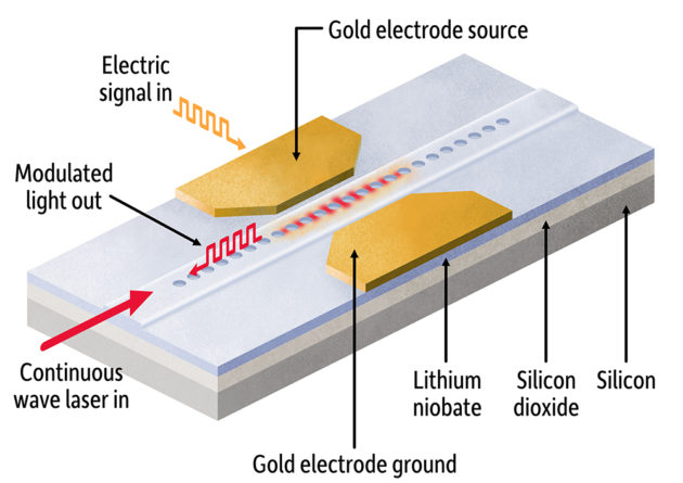
Step into the cutting edge of light-based technology with Photonics Revolution: A Comprehensive Guide to Material Platforms for Photonic Integrated Circuits (PICs). In this course, you’ll discover how harnessing photons instead of electrons is transforming everything from ultra‑fast data centers to next‑generation sensors and quantum computers. Beginning with an intuitive introduction to photonics and PICs, you’ll explore the material building blocks—silicon, III‑V semiconductors, polymers, graphene, and beyond—that make these laser‑powered chips possible. Through real‑world case studies and design deep‑dives, you’ll see how advances in materials science are unlocking groundbreaking new devices and applications.

Over the span of this course, you’ll master the fundamentals of waveguide design, fabrication techniques like photolithography and wafer bonding, and strategies for thermal management and hybrid integration. You’ll then dive into high‑impact applications—optical interconnects in data centers, biochemical sensing on a chip, and even quantum photonics for secure communication and precision metrology. Whether you’re an engineer eager to build the next PIC, a researcher pushing material frontiers, or simply curious about the future of light‑based electronics, this guide will equip you with the knowledge and practical insights to lead the photonics revolution.

Show More

What Will You Learn?

  • Grasp the physics of photonics and the architecture of PICs
  • Compare material platforms: silicon, III‑V compounds, polymers, silicon nitride, and graphene
  • Design optimized waveguides, modulators, and detectors for high‑performance PICs
  • Apply fabrication methods like lithography, etching, and wafer bonding
  • Integrate and package components while managing heat and power efficiency
  • Characterize and test PIC devices using optical and electrical metrology
  • Explore optical communication systems in data centers and long‑haul networks
  • Implement PIC‑based biochemical, environmental, and quantum sensors
  • Understand challenges in scalability, hybrid integration, and emerging materials
  • Anticipate future trends in materials and manufacturing for next‑gen PICs

Course Content

Introduction to Photonics and Photonic Integrated Circuits (PIC)
Photonics harnesses light—rather than electrons—as the information carrier, enabling blisteringly fast data transmission, sensing, and signal processing. Photonic Integrated Circuits (PICs) miniaturize optical components—waveguides, modulators, detectors—onto a single chip, much like electronic ICs do for electrons. This integration slashes size, weight, and power consumption, while boosting bandwidth and reliability. From high‑speed data centers to lab‑on‑a‑chip sensors, PICs are revolutionizing telecommunications, biomedical diagnostics, environmental monitoring, and burgeoning fields like quantum information.

  • What is Photonics?
    00:00
  • Overview of Photonic Integrated Circuits (PIC)
    00:00
  • Importance and Applications of PICs
    00:00

II. Fundamentals of Material Platforms for PICs
The choice of substrate material defines PIC performance. Silicon photonics leverages CMOS‑compatible fabrication for dense, low‑cost integration but faces challenges in efficient light emission. III‑V compound semiconductors (e.g., InP, GaAs) offer direct bandgaps for lasers and amplifiers, though integration with silicon demands complex bonding. Emerging platforms—polymer‑based, silicon nitride, III‑V on silicon, and graphene—promise unique advantages: flexibility, ultra‑low loss, hybrid functionality, and extreme electro‑optical tunability, opening the door to highly customized PICs for specialized applications.

A. Silicon Photonics
Silicon photonics leverages mature CMOS fabrication to create low-cost, high‑volume PICs, integrating photonic devices alongside traditional electronics. Silicon’s high refractive index contrast enables compact waveguides and tight bends, but its indirect bandgap makes on‑chip lasers challenging. Design considerations include managing propagation loss and thermal tuning, while fabrication relies on advanced lithography, etching, and wafer‑scale processes to achieve sub‑100 nm feature sizes.

B. III-V Compound Semiconductors
III‑V materials (InP, GaAs, GaN) offer direct bandgaps for efficient light emission, optical gain, and high‑speed modulation—key for lasers and amplifiers in PICs. Fabrication typically involves epitaxial growth, wafer bonding to silicon substrates, and precision etching. Designers must balance optical confinement with material strain and thermal expansion mismatches, making integration with silicon a complex but rewarding route to hybrid photonic–electronic chips.

C. Other Emerging Material Platforms
Polymer‑based PICs offer flexibility, low‑temperature processing, and large‑area patterning—but suffer higher loss than silicon. Silicon nitride combines ultra‑low optical loss with CMOS compatibility, ideal for nonlinear optics and frequency comb generation. III‑V on silicon merges the best of both worlds: efficient light sources on a silicon backbone. Graphene’s extreme electro‑optical tunability and broadband absorption pave the way for modulators and photodetectors with unprecedented speed and compactness.

III. Design and Fabrication Techniques for Material Platforms
Designing a high‑performance PIC requires careful waveguide optimization to minimize loss and dispersion, strategic component integration and packaging to ensure optical alignment and environmental protection, and robust thermal management schemes to stabilize performance. Fabrication employs photolithography, etching and deposition to sculpt nanoscale features; wafer bonding techniques to hybridize dissimilar materials; and rigorous testing and characterization—from near‑field scans to spectral analysis—to validate device behavior before deployment.

A. Design Considerations for PICs
PIC design begins with precise waveguide engineering to minimize scattering loss and dispersion, often using rib or strip geometries optimized via simulation. Component integration and packaging demand alignment of optical fibers, thermal stabilization, and hermetic sealing. Thermal management, via integrated heaters or heat‑spreading layers, ensures wavelength stability and prevents performance drift in dense PIC assemblies.

B. Fabrication Techniques for Material Platforms
Building PICs employs photolithography to define patterns, dry or wet etching to sculpt waveguides and devices, and deposition (PECVD, sputtering) for claddings and active layers. Wafer bonding (e.g., adhesive or fusion) enables heterogeneous integration of disparate materials. Rigorous testing and characterization—optical loss measurements, near‑field imaging, and spectral analysis—validate device performance before packaging and deployment.

IV. Applications of Material Platforms in PICs
Material‑tailored PICs underpin optical communication systems, enabling terabit‑scale data‑center interconnects and long‑haul fiber‑optic networks with minimal latency and power. In sensing and metrology, PICs provide highly sensitive biochemical and medical assays, environmental pollutant detection, and precision length or refractive index measurements on a chip. The quantum frontier leverages PICs for quantum computing (photon‑based qubits and gates), quantum communication (secure key distribution), and quantum sensing (e.g., ultraprecise timekeeping and field sensing), all benefiting from material‑engineered devices.

A. Optical Communication Systems
Material‑optimized PICs are the backbone of data‑center interconnects, supporting multi‑terabit links with minimal latency and energy use. In optical networking, PICs enable reconfigurable switches, coherent transceivers, and wavelength‑division multiplexers for long‑haul fiber‑optic links, enhancing bandwidth and reach while reducing cost and footprint.

B. Sensing and Metrology
PICs unlock compact biochemical sensors for point‑of‑care diagnostics, detecting biomarkers via evanescent‑field interactions. Environmental sensing chips monitor air or water quality by measuring refractive‑index changes. Optical metrology PICs provide on‑chip interferometers and spectrometers for industrial process control and precision measurement in manufacturing.

C. Quantum Photonics
In quantum computing, PICs host single‑photon sources, beam splitters, and detectors for scalable qubit manipulation. Quantum communication leverages PIC‑based entangled‑photon generators and integrated modulators for secure key distribution. Quantum sensing uses on‑chip interferometers for ultraprecise timekeeping, gravimetry, and electromagnetic field measurements.

V. Challenges and Future Directions
Scaling PIC technology faces hurdles in integration density, interconnecting diverse materials, and managing heat in ever‑smaller footprints. Improving power efficiency and mitigating thermal dissipation are critical as on‑chip light sources and amplifiers proliferate. Hybrid integration—combining silicon with III‑V or 2D materials—offers a path forward, supported by ongoing advances in novel materials and manufacturing processes like 3D photonic printing. The road ahead promises even tighter integration of electronics and photonics, new low‑loss materials, and fully heterogeneous platforms that drive the photonics revolution toward new applications and markets.

VI. Conclusion
In summary, mastering the material platforms for PICs is essential to unlocking light‑based technologies that outperform electronics in speed, bandwidth, and functionality. From silicon to III‑V, polymers to graphene, each material platform brings unique strengths and challenges that shape device design, fabrication, and application. As you move forward, the interplay of materials science, nanofabrication, and system‑level engineering will define the next wave of photonic innovations—reshaping communications, sensing, computing, and beyond.

wpChatIcon
    wpChatIcon